September 10, 2026 | By KJLC Blog
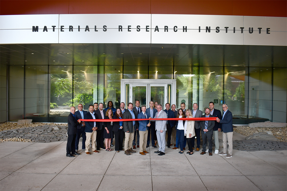
The Kurt J. Lesker Company and Penn State University have launched the Kurt J. Lesker Company Atomic Scale Processing Center of Excellence (ASPIRE), housed in Penn State's Nanofabrication Laboratory at the Millennium Science Complex. ASPIRE pairs KJLC's atomic layer deposition (ALD) and atomic layer etching (ALE) equipment with Penn State's research and characterization infrastructure to develop and validate atomic-scale processing recipes for semiconductor, quantum, photonic, and advanced packaging technologies recipes that will ultimately be shared with KJLC customers and academic researchers.
Read More
Tags:
Systems
Vacuum Science
Deposition Techniques
News
June 26, 2026 | By KJLC Innovate
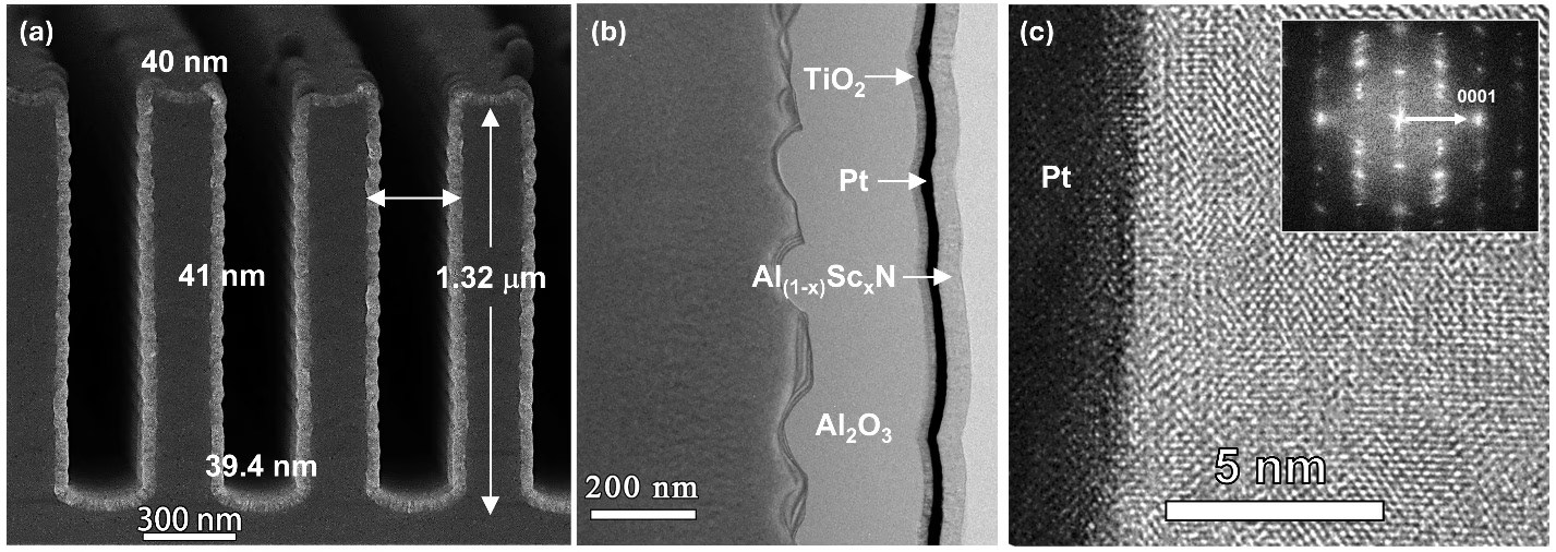
From high-purity thin films to functional ferroelectrics in 3D architectures.
As semiconductor devices continue to evolve toward atomic-scale dimensions and complex 3D architectures, the requirements placed on materials are becoming increasingly stringent. Thin films must not only be conformal and uniform—they must also deliver functional properties at the atomic level, with impurity concentrations reduced to near-zero.
Read More
Tags:
INNOVATE
Systems
Vacuum Science
Deposition Techniques
April 24, 2026 | By KJLC Blog
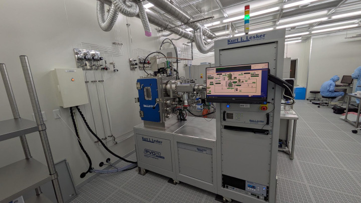
The Okinawa Institute of Science and Technology (OIST), located in Okinawa, Japan, is known for its interdisciplinary approach to research and its investment in advanced scientific infrastructure. From nanofabrication to materials characterization, OIST's core facilities are designed to support researchers as they push the boundaries of discovery.
Read More
Tags:
INNOVATE
Systems
Vacuum Science
Deposition Techniques
February 13, 2026 | By KJLC Innovate
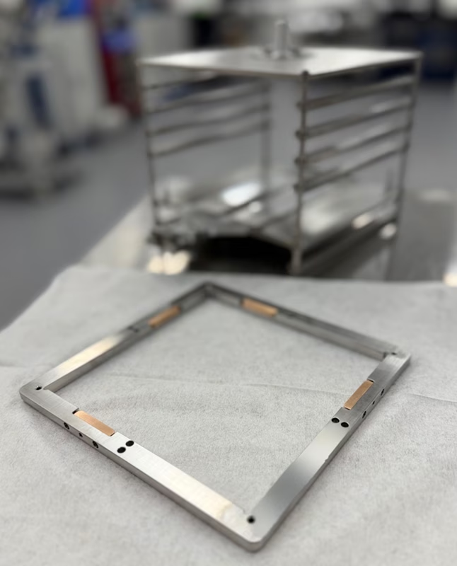
In the evolving landscape of advanced materials discovery and thin film device fabrication, precision and repeatability are critical to innovation. One widely adopted method for patterning and selective deposition is the use of shadow masks—physical stencils that define regions on a substrate where material is deposited. While this approach enables rapid prototyping, device isolation, and high-throughput fabrication, it also introduces challenges in mask alignment, resolution control, and system contamination—especially when used in combinatorial materials science.
Read More
Tags:
INNOVATE
Systems
Vacuum Science
Deposition Techniques
October 07, 2025 | By KJLC Innovate
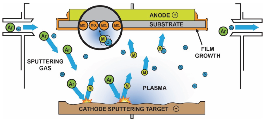
Plasma processes, especially reactive magnetron sputtering, have become foundational in the production of advanced thin film coatings across industries ranging from microelectronics to optics and energy. Yet, the inherent complexity and dynamism of plasma environments present significant challenges for process stability, film quality, film reproducibility, and throughput. Plasma Emission Monitoring (PEM) has emerged as a transformative analytical and control technique, enabling precise regulation of plasma chemistry during deposition. This article explores the principles, challenges, and industrial impact of this real-time, in situ characterization method for reactive magnetron sputtering.
Read More
Tags:
INNOVATE
Systems
Vacuum Science
Deposition Techniques
August 11, 2025 | By KJLC Innovate
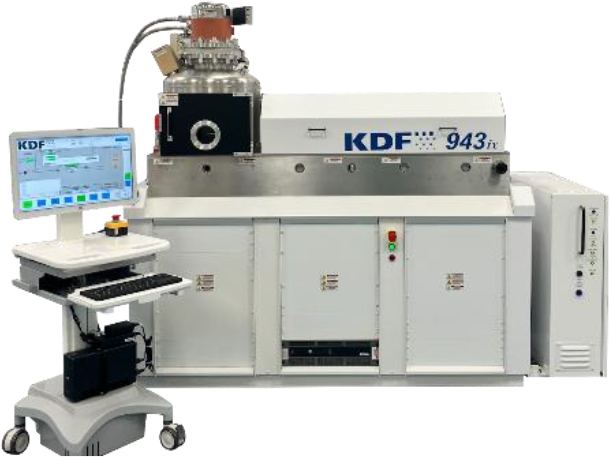
Metallic coatings deposited using the KDF Enhanced Rotating Planetary Pallet (ERPP) exhibit exceptionally high film uniformity and tight process repeatability. This performance is driven by the synergistic effect of the concomitance of the planetary revolution and the system's standard linear scanning mode. KDF Technologies has developed both reactive and non-reactive sputtering processes for metallic, semi-metallic, semiconductor, and dielectric materials. These processes consistently achieve film uniformity better than ±1% across the pallet, with repeatability exceeding ±0.5% from pallet to pallet. With this capability, we ensure high-performance processing of multilayer conductive barriers and contact materials essential for integrated circuits, in addition to delivering premium titanium tungsten films for adhesion and diffusion applications in both microelectronics and decorative technologies. Furthermore, the flexible programmability of the rotating motion will be examined in the context of its impact on improving deposition uniformity and tailoring surface morphology. With the ongoing evolution of thin-film device applications, deposition tools must meet progressively tighter specifications, delivering superior film uniformity and process repeatability to support next-generation performance.
Read More
Tags:
INNOVATE
Systems
Vacuum Science
Deposition Techniques
July 31, 2025 | By KJLC Innovate

As semiconductor and microelectronic devices evolve, requiring atomic-scale manufacturing precision, the purity constraints on materials become extreme. At the 2nm node in semiconductor development, line widths are on the order of 40 atoms! Among the more interesting materials is the ferroelectric material aluminum scandium nitride (AlScN), a wurtzite-structured, solid solution material that combines the superior piezoelectric properties of AlN with the ferroelectric behavior introduced through scandium doping. AlScN has demonstrated breakthrough potential for nonvolatile memory, energy harvesting, microelectromechanical systems (MEMS), Rf filters, and optical devices. All of the applications require conformal, ultra-pure thin films with atomic-level precision.
Read More
Tags:
INNOVATE
Systems
Vacuum Science
Deposition Techniques
July 25, 2025 | By KJLC Innovate
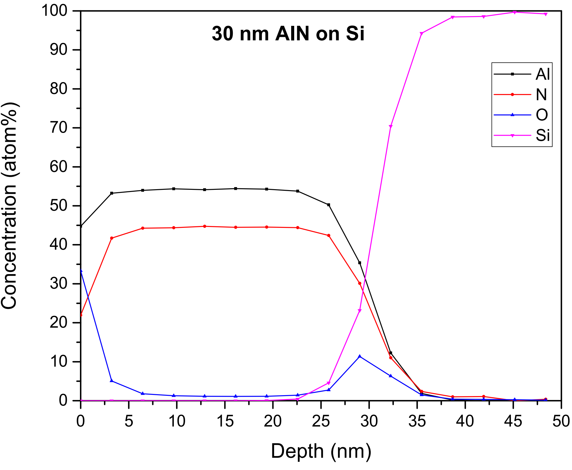
Jeffrey R. Shallenberger of the Materials Research Institute at Penn State University has led a groundbreaking study demonstrating the detection of trace oxygen levels—down to 0.1 atomic percent—in highly reactive thin films using X-ray Photoelectron Spectroscopy (XPS). This work sets a new benchmark for precision in surface analysis and thin film quality control.
Read More
Tags:
INNOVATE
Systems
Vacuum Science
Deposition Techniques
July 15, 2025 | By KJLC Innovate
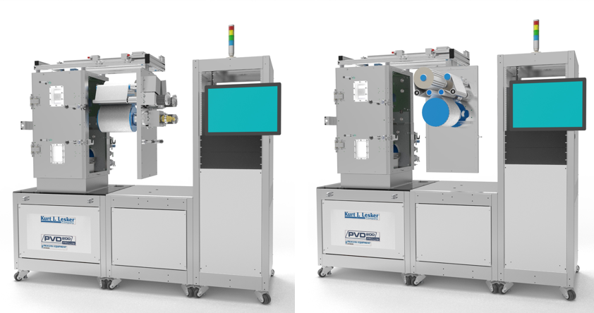
The Kurt J. Lesker Company is proud to announce the launch of the Pro Line Roll-to-Roll (R2R) Module, a transformative enhancement to the industry-leading Pro Line PVD 200 Thin Film Deposition System. This new, cost-effective, drop-in module brings true roll-to-roll coating capability to the PVD 200 platform, empowering researchers and product developers to bridge the gap between laboratory-scale experimentation and scalable pilot production of flexible electronic devices.
Read More
Tags:
INNOVATE
Systems
Vacuum Science
Deposition Techniques
April 08, 2025 | By KJLC Innovate
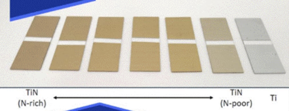
In the high-stakes world of thin film deposition, especially for functional oxides, nitrides and other compounds made by reactive sputtering with metals, precision is everything.
Read More
Tags:
INNOVATE
Systems
Vacuum Science
Deposition Techniques
Previous Entries


