March 15, 2019 | By KJLC Innovate
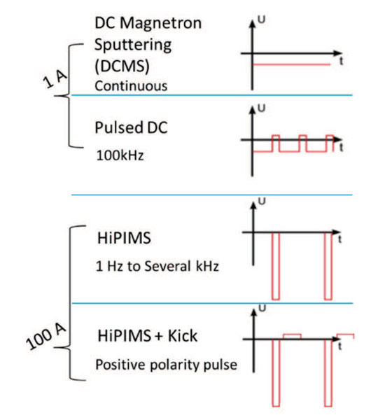
High impulse power magnetron sputtering, either HIPIMS or HiPMS, was first reported in 1999 by Dr. Vladimir Kouznetsov, et al. from Linköping University’s Department of Physics. HIPIMS is distinct from classical direct current magnetron sputtering, or dcMS, because it utilizes a rapid series of pulses at very high voltage, on the order of 2000V, and high current density approaching 10A/cm2. In addition, HIPIMS also exhibits some degree of self-sputtering, where sputter target adatoms are ionized with some recycling of process gas and ionized target material to the surface of the target.
Read More
Tags:
INNOVATE
Vacuum Science
May 09, 2018 | By KJLC Innovate
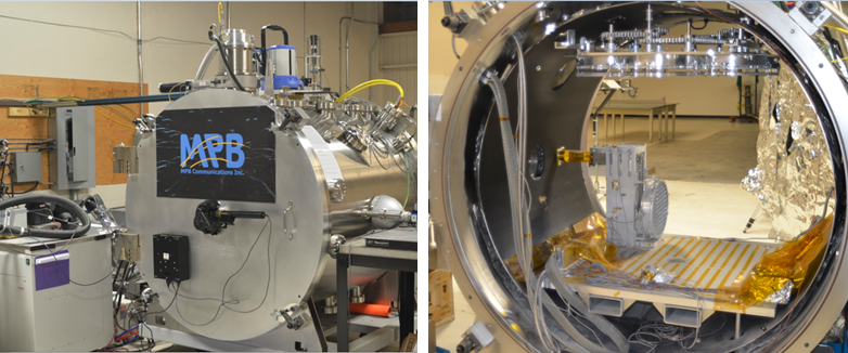
The current push to commercialize space travel has resulted in renewed demand to launch objects and even people into earth orbit or event deep space. Companies including SpaceX, Blue Origin and Rocket Lab have demonstrated the ability to make certain portions of a launch vehicle reusable and that may dramatically alter the cost to get to space. True rocket ship factories are emerging which, in one case, can put out a couple of full blown launch vehicles every month!
Read More
Tags:
INNOVATE
Systems
Vacuum Science
Deposition Techniques
April 11, 2018 | By KJLC Innovate

Researchers Dr. André Anders and Dr. Yuchen Yang have expanded on their previous imaging work on linear magnetron cathodes. In their most recent work, titled “Plasma studies of a linear magnetron operating in the range from DC to HIPIMS,” the authors put forth additional information on the evolution and movement of spokes with several deposition materials and discharge conditions.
Read More
Tags:
INNOVATE
Vacuum Science
November 28, 2017 | By KJLC Innovate
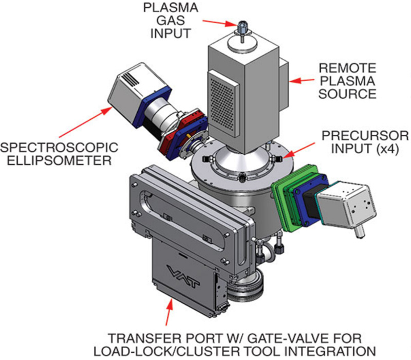
The Kurt J. Lesker Company® (KJLC®), a global manufacturer of vacuum systems, thin film deposition tools and vacuum components, today announced that the United States Patent and Trademark Office has issued US patent number 9,695,510, 'Atomic Layer Deposition Apparatus and Process', covering the design of an atomic layer deposition system and the process to use that system to deposit highly precise and conformal thin films. This proprietary technology substantially reduces the interaction of various precursor gas molecules with the internal surfaces of the reaction chamber and enables actual focusing of gas streams to more effectively coat the surface of arbitrarily large substrates.
Read More
Tags:
INNOVATE
Systems
Vacuum Science
Deposition Techniques
October 25, 2017 | By KJLC Innovate

In a July 2017 publication, Drs. André Anders and Yuchen Yang provide an enhanced description of the flows and energy of electrons at the face of a magnetron sputter cathode. By combining a unique imaging process and a linear cathode (target) the researchers were able to generate a series of time/space images which shows plasma instabilities driven by the motion of electrons, within the cathode's magnetic field. The images show the effects on plasma flow for both conventional DC magnetron sputtering (dcMS) and also high power impulse magnetron sputtering (HiPIMs). The full paper is available on line at http://aip.scitation.org/doi/10.1063/1.4994192.
Read More
Tags:
INNOVATE
Vacuum Science
Deposition Techniques
February 20, 2017 | By KJLC Innovate
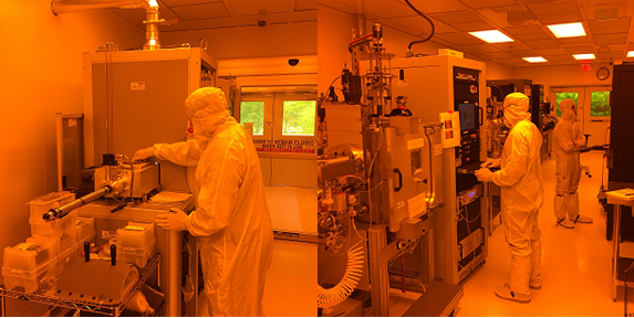
Next generation vacuum deposition systems must evolve in order to keep pace with the ongoing evolution of thin film materials and devices. Researchers seeking to pursue new areas, such as biomedical devices, 2D materials, specialized magnetics and oxide-based films need new tools to support their work. The frontiers of materials science, particularly at the intersection of biology and thin film deposition, have brought new materials into the vacuum space that were never intended to be there.
Read More
Tags:
INNOVATE
Systems
Vacuum Science
Deposition Techniques
August 30, 2016 | By KJLC Innovate
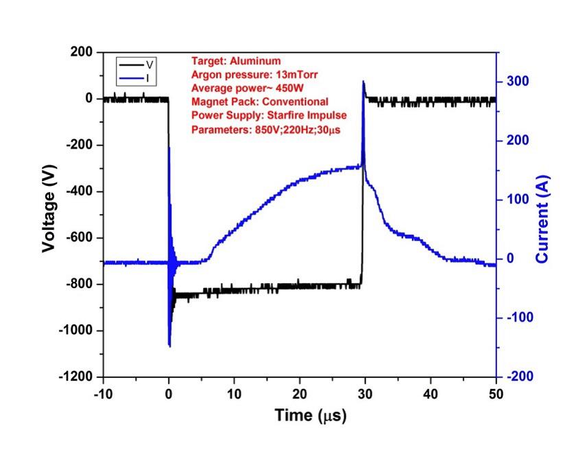
High Power Pulsed Magnetron Sputtering (HPPMS) or High Power Impulse Magnetron Sputtering (HIPIMS) is a type of magnetron sputtering technique where high power pulses of hundreds of microseconds are applied to the magnetron target at frequencies ranging from a few Hz to several kHz.
Read More
Tags:
INNOVATE
Systems
Vacuum Science
July 20, 2016 | By KJLC Innovate
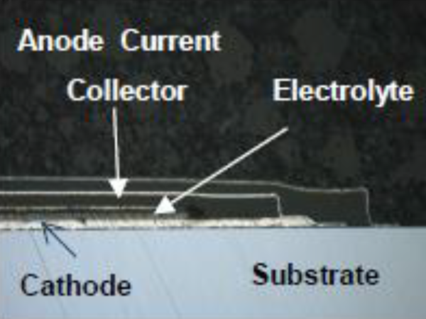
The concept of energy storage in thin films has been around for a long time. One of the early uses of the term 'Thin Film Battery' (TFB) was in a 1976 patent by Exxon [1]. Nearly 20 years later, Bates and his team at Oak Ridge National Laboratory (ORNL) patented the sputter-based, all solid state battery utilizing the electrolyte LiPON [2]. The Bates battery paired LiCoO2 and Li3PO4-xNx (LiPON) to produce a 4 volt secondary cell.
Read More
Tags:
INNOVATE
May 13, 2016 | By KJLC Innovate

Solar cells work by using materials that absorb photons from sunlight in a broad spectral range and in turn effectively convert this captured light into free charges that produce electricity. Modern solar cells are based on crystalline Silicon (c-Si) which is a cheap and abundant semiconductor, however the cost to produce electricity using them is relatively high as the efficiency rates of c-Si based cells are relatively low. As a result thin film solar cells have been developed to combat crystalline Silicon's inherent inefficiencies. Technologies such as CIGS, CdTE, amorphous Silicon and OPV have all strived to create solar cells that have high efficiencies coupled with good cell stability and low manufacturing costs.
Read More
Tags:
INNOVATE
Systems
Vacuum Science
May 09, 2016 | By KJLC Innovate

ALD has been described as a thin film deposition technology that can keep the semiconductor industry on track per Moore's law (or observation) [1] for a few more years. In its most ideal form, it is a process that enables monolayer, or sub-monolayer growth of certain materials through the sequential exposure of a functionalized substrate to a pair of precursor gases. If dosed correctly the gases attach at specific surface sites and react to create a near perfect film on the order of a few angstroms thick. Presently the U.S. Department of Defense anticipates that the last process node for semiconductor devices (the end of Moore's) is 7 nm and will be achieved by 2020 [2].
Read More
Tags:
INNOVATE
Systems
Vacuum Science
Deposition Techniques
Previous Entries
Next Entries