


CUSTOMER RESEARCH FEATURE
How an ultrathin buffer layer and integrated inert-atmosphere processing helped address a critical electrode-integration challenge in high-efficiency photovoltaics.

An approximately 3 nm AlOₓ buffer, deposited in 38 thermal atomic layer deposition cycles, protected the underlying device during pulsed-DC indium tin oxide sputtering. The resulting architecture supported semi-transparent perovskite cells above 17% efficiency and monolithic perovskite-silicon tandem cells above 26%.
Perovskite-silicon tandem solar cells offer a pathway beyond the practical efficiency limits of conventional silicon photovoltaics. Translating record laboratory performance into manufacturable devices, however, requires every layer in the tandem stack to be deposited without damaging the sensitive materials beneath it.
One particularly difficult step is the deposition of the transparent conductive oxide electrode. Indium tin oxide (ITO) combines high optical transparency with low electrical resistance, but energetic species generated during magnetron sputtering can damage the underlying charge-transport and perovskite layers.
Researchers from the Institute for Photovoltaics at the University of Stuttgart, together with collaborators from Forschungszentrum Jülich, INL Braga, and AIKO Europe, demonstrated that an approximately 3 nm atomic-layer-deposited aluminum oxide (AlOₓ) buffer can provide effective protection during ITO sputtering while supporting high-performance semi-transparent and perovskite-silicon tandem devices.



The electrode-integration challenge
Transparent conductive oxides (TCOs) are essential in semi-transparent perovskite solar cells and monolithic perovskite-silicon tandem devices. They must provide low electrical resistance while transmitting as much useful light as possible.
Magnetron sputtering is a well-established physical vapor deposition (PVD) process for producing uniform, high-quality TCO coatings over large areas. However, energetic ions and neutral species generated during sputtering can interact with underlying charge-transport and perovskite layers, creating defects and degrading device performance.
Sputtering-induced damage can contribute to:
- Increased non-radiative recombination
- Loss of open-circuit voltage
- Reduced fill factor and power-conversion efficiency
- Potential degradation of device stability
Protective buffer layers are therefore commonly placed between the electron-transport layer and the sputtered TCO. Tin oxide (SnOₓ) is widely used, but reliable protection can require comparatively thick films, increasing deposition time and precursor use.
An ultrathin ALD protection layer
The Stuttgart team investigated whether AlOₓ deposited by atomic layer deposition (ALD) could provide robust sputter protection at substantially lower thickness. Thermal ALD was used to deposit AlOₓ directly onto the C₆₀ electron-transport layer before ITO deposition by pulsed-DC magnetron sputtering.
The optimum AlOₓ thickness was approximately 3 nm, corresponding to 38 ALD cycles. The ALD-grown film formed a dense, conformal coating that protected the underlying device stack during sputtering. In the reported comparison, thin SnOₓ films more frequently showed incomplete coverage and pinhole formation.
Figure 1 compares the surface morphology and coverage of the perovskite/C₆₀ stack with SnOₓ and AlOₓ buffer layers and illustrates the different ALD growth behavior.
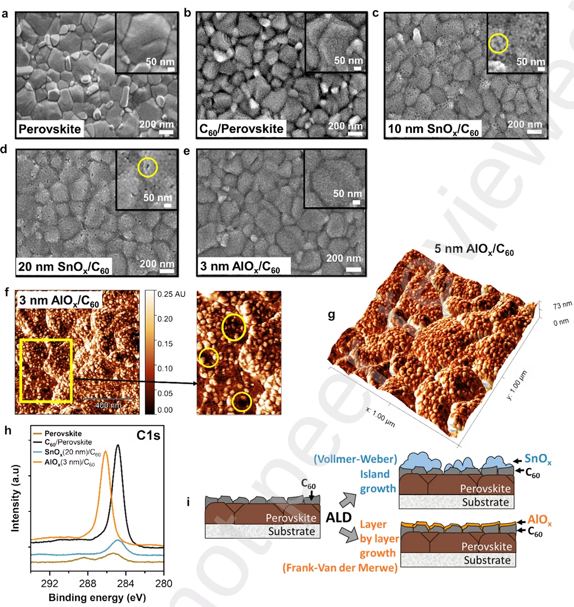
Aluminum oxide is normally regarded as an electrical insulator, making its successful use at this interface particularly significant. At an ultrathin thickness of approximately 3 nm, the layer provided physical protection while the completed device retained effective charge extraction. A specific transport mechanism should not be assumed unless directly established by the study.
Why 3 nm matters
Within the device architecture and process conditions investigated, the approximately 3 nm AlOₓ layer provided effective sputter protection compared with an approximately 20 nm SnOₓ buffer layer. This represents an approximately 85% reduction in nominal buffer-layer thickness.
The result demonstrates a central strength of ALD: film thickness and coverage can be controlled at the nanometre scale, allowing a functional protection layer to be engineered with substantially fewer deposition cycles. For photovoltaic researchers and process engineers, thinner functional layers may reduce precursor use and process time while preserving device performance.
Device performance
Semi-transparent perovskite solar cells incorporating the ultrathin AlOₓ protection layer achieved power-conversion efficiencies above 17%. Monolithic perovskite-silicon tandem devices exceeded 26%, with independent reporting citing a tandem efficiency of approximately 26.9%.
Figure 2 summarizes the semi-transparent device architecture and compares the J-V parameters obtained with buffer-free, SnOₓ-buffered, and AlOₓ-buffered devices.
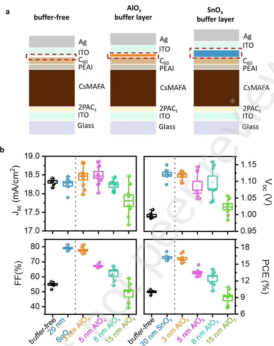
The AlOₓ layer was not the sole source of the reported device efficiency. Its contribution was to enable integration of the sputtered ITO electrode while limiting damage to the sensitive underlying structure.
The study therefore shows that carefully engineered ALD buffer layers can:
- Protect sensitive device layers during sputtering
- Maintain effective charge extraction
- Reduce nominal buffer-layer thickness
- Support high-performance semi-transparent and tandem architectures
Initial thermal-stress comparison
In an initial thermal-stress comparison, devices were held at 85 °C in dry air for four hours. The AlOₓ-buffered devices showed approximately 1.6% relative efficiency loss, compared with approximately 8.0% for devices using the SnOₓ buffer.
This short-duration test should not be interpreted as a demonstration of long-term module reliability. It does, however, indicate that the ultrathin AlOₓ layer did not introduce an obvious thermal-stability penalty under the conditions evaluated. Longer-duration and application-relevant reliability studies would be needed to assess commercial lifetime.
Integrated processing for air-sensitive device stacks
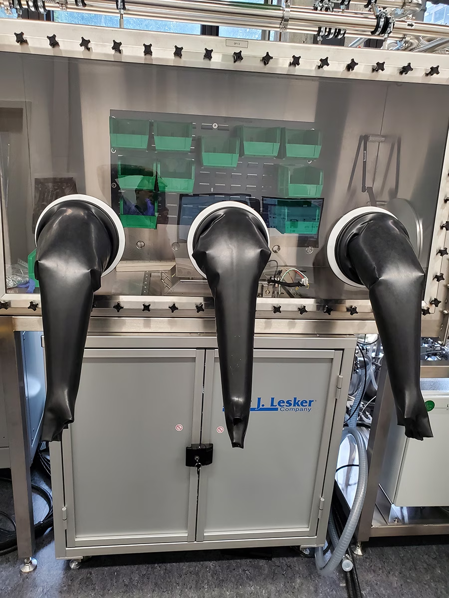
The devices were fabricated using an integrated inert-atmosphere processing platform supplied by the Kurt J. Lesker Company. The system connects solution processing, thermal evaporation, ALD, and sputtering capabilities through glovebox environments, allowing sensitive samples to move between key process stages without exposure to ambient air.
The ultrathin AlOₓ layers were deposited using a glovebox-integrated KJLC ALD150LE before transfer to the sputtering process. This controlled workflow helped the research team investigate the buffer layer while preserving sensitive interfaces within the device stack.
The work illustrates a broader requirement in advanced photovoltaic research: new materials must be developed alongside practical methods for integrating them into increasingly complex device architectures. Combining complementary deposition technologies within a controlled environment gives researchers a flexible platform for studying those interactions.
A practical route through a critical integration problem
This work demonstrates how atomic-scale processing can address a practical integration challenge in perovskite-silicon tandem solar cells. An approximately 3 nm ALD-grown AlOₓ layer protected the underlying device during ITO sputtering while allowing the completed architecture to retain effective charge extraction.
Just as importantly, the study shows the value of connecting complementary deposition technologies within a controlled inert environment. For air-sensitive photovoltaic materials, moving between evaporation, ALD, and sputtering without ambient exposure allows researchers to investigate complex interfaces with greater process control.
As tandem photovoltaic architectures develop, progress will depend not only on new absorber materials but also on reliable ways to integrate every functional layer. This research provides a strong example of materials innovation and deposition-process integration working together to reduce one important barrier to future scalable manufacturing.
This preprint presents the study behind the results featured here, including the development of an approximately 3 nm ALD-grown AlOₓ buffer layer to protect sensitive perovskite device stacks during ITO sputtering. It provides further detail on the layer’s growth, device integration, performance, and initial thermal-stress comparison.
Materials Today: Sputter-resistant ultrathin aluminum oxide layer enables robust perovskite tandem solar cells