


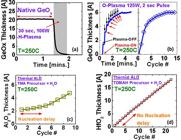
Germanium (Ge) is a promising candidate to enhance p-channel metal oxide silicon field transistor (MOSFET) device performance. The successful development of Ge-based field effect devices requires the integration of a high-quality dielectric with equivalent oxide thickness (EOT) less than 1 nanometer that forms an electrically well behaved semiconductor dielectric interface. Although GeOx/Ge has been found promising, the thermodynamic instability as well as the relatively low dielectric constant of GeOx requires an alternative approach. The utilization of an ultrathin Si layer, to modify the semiconductor-dielectric interface from Ge into Si, is a viable approach that has been successfully demonstrated; however, the introduction of a thin Si layer into the gate stack is incompatible with the 3D FinFET manufacturing process flow and also leads to increased EOT. It is, therefore, desirable to develop a multilayer gate-stack by atomic layer deposition (ALD), where an ultrathin GeOx layer can be thermodynamically stabilized and combined with a high-k dielectric film to meet the stringent requirement of low interface trap density and large capacitance density while maintaining a low gate leakage under the constraint of full compatibility with modern 3D FinFET geometries.
Read More