




From high-purity thin films to functional ferroelectrics in 3D architectures.
As semiconductor devices continue to evolve toward atomic-scale dimensions and complex 3D architectures, the requirements placed on materials are becoming increasingly stringent. Thin films must not only be conformal and uniform—they must also deliver functional properties at the atomic level, with impurity concentrations reduced to near-zero.
Among the most promising materials for next-generation devices is aluminum–scandium nitride (AlScN), a wurtzite-structured alloy that combines strong piezoelectric response with ferroelectric switching behavior. This combination makes AlScN a leading candidate for applications in:
- Nonvolatile memory
- RF filters and resonators
- PiezoMEMS devices
- Advanced sensing technologies
In a recent publication in a Nature Portfolio journal, researchers from Kurt J. Lesker Company (KJLC), in collaboration with Army Research Laboratory, Massachusetts Institute of Technology, and Penn State University, report a world-first demonstration of ferroelectric AlScN grown by plasma-enhanced atomic layer deposition (PEALD) under ultrahigh purity conditions (UHP-C).
From High Purity to Functional Ferroelectrics
In earlier work, KJLC demonstrated that achieving ultra-high purity conditions (UHP-C) in ALD was critical to unlocking the full potential of AlScN. Impurities such as oxygen and carbon—commonly present in traditional deposition approaches—have been shown to degrade ferroelectric performance, increase leakage currents, and broaden switching behavior.
By combining:
- Advanced vacuum system design
- High-purity precursor delivery
- Plasma-enhanced ALD chemistry
The UHP-C approach minimizes contamination to near detection limits for X-ray photoelectron spectroscopy (XPS), enabling films with significantly improved electrical performance.
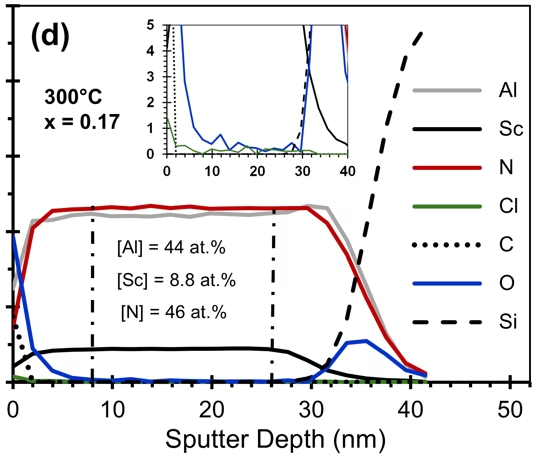
The newly published work builds directly on this foundation—moving beyond material quality to demonstrate true ferroelectric functionality in ALD-grown AlScN.
Enabling Ferroelectric AlScN by ALD
The breakthrough centers on a supercycle PEALD process that alternates between AlN and ScN growth steps, allowing precise control of film composition and structure at the atomic scale.
This process enables:
- Layer-by-layer control of composition (Al1-xScxN)
- Formation of highly ordered wurtzite crystal structure
- Integration with plasma activation to enhance nitride formation
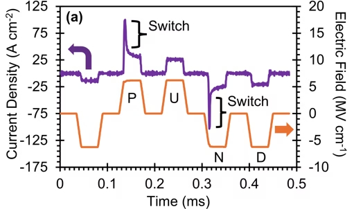
Most importantly, the films exhibit clear ferroelectric switching behavior, marking a critical milestone for ALD-based nitride materials.
3D Conformality: A Key Advantage of ALD
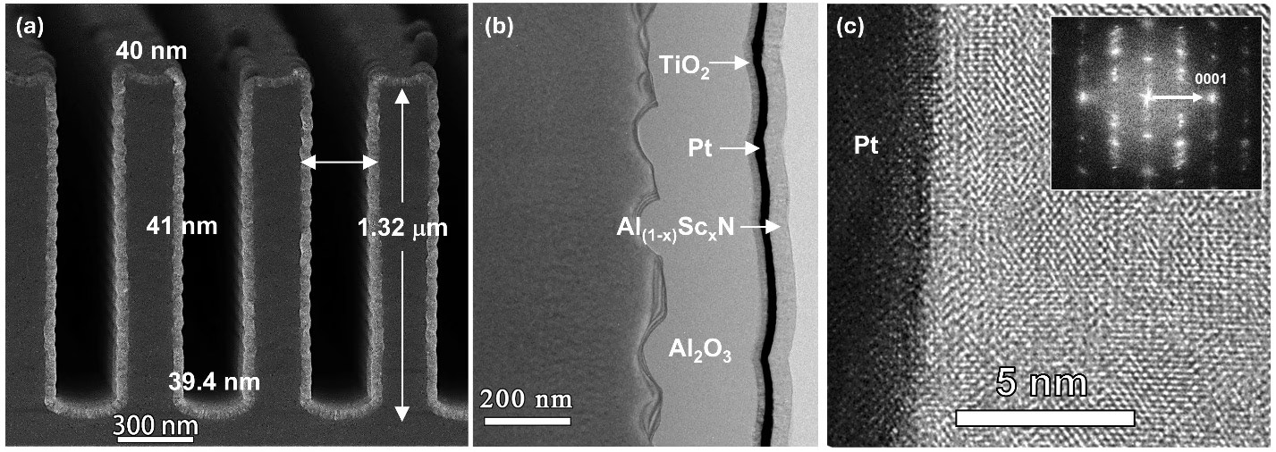
One of the most significant outcomes of this work is the demonstration of highly conformal AlScN films across complex 3D features.
Cross-sectional imaging shows:
- Uniform coating along trench top, sidewalls, and bottom
- Minimal thickness variation across high-aspect-ratio structures
- Crystalline structure maintained even on sidewall surfaces
This level of conformality is not achievable with traditional line-of-sight deposition methods such as sputtering or MBE, and is essential for enabling:
- 3D ferroelectric memory architectures
- Advanced MEMS structures
- Embedded functional materials in nanoscale devices
Structural Order and Epitaxial Growth
In addition to conformality, the PEALD-grown films demonstrate:
- Strong c-axis alignment on platinum substrates
- Epitaxial growth on GaN, with excellent crystalline quality
- Preservation of polarization direction throughout 3D structures
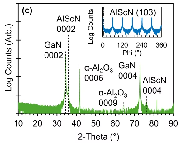
These results confirm that ALD can produce not just conformal films—but device-quality crystalline materials suitable for advanced applications.
The Role of Ultrahigh Purity Conditions (UHP-C)
The success of this work is directly tied to KJLC's UHP-C process environment, which integrates ultra-high vacuum principles with advanced gas purification and delivery systems.
Key benefits include:
- Suppression of oxygen and carbon contamination
- Improved crystallinity and film density
- Reduced leakage and enhanced ferroelectric performance
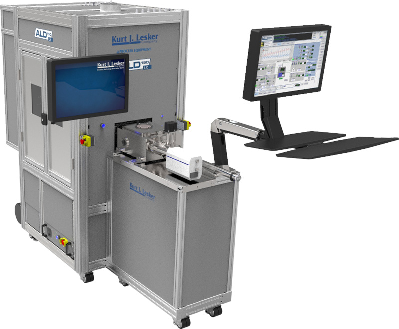
The ALD150LX platform, configured for UHP-C operation, provides a scalable and production-relevant solution for the development of advanced nitride materials.
A Platform for Next-Generation Materials
This demonstration of ferroelectric AlScN by PEALD represents more than a single material breakthrough—it establishes a new paradigm for ALD as a functional materials platform.
As device architectures continue to evolve, the need for...
- Conformal deposition in 3D
- Atomic-scale composition control
- Ultra-low impurity levels
will only increase.
The UHP-C PEALD approach is expected to enable not only AlScN, but a broader class of multicomponent nitrides and advanced functional thin films.
Driving the Future of Semiconductor Innovation
This publication highlights the power of close collaboration between industry, academia, and government research organizations in advancing semiconductor technology.
It also reflects an important evolution for Kurt J. Lesker Company.
By combining expertise in:
- Vacuum science and engineering
- Thin film deposition platforms
- Advanced materials development
KJLC is moving beyond traditional equipment supply toward delivering integrated solutions that enable next-generation devices.
Learn More
The full publication, "Ferroelectric Aluminum–Scandium Nitride by Plasma-Enhanced Atomic Layer Deposition under Ultrahigh Purity Conditions," is now available in a Nature Portfolio journal.
To learn more about KJLC's ALD capabilities and UHP-C platform, visit our website or contact the Atomic Scale Processing team.