











Application Specific Systems
PURPOSE-BUILT FOR PIONEERING RESEARCH
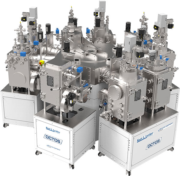
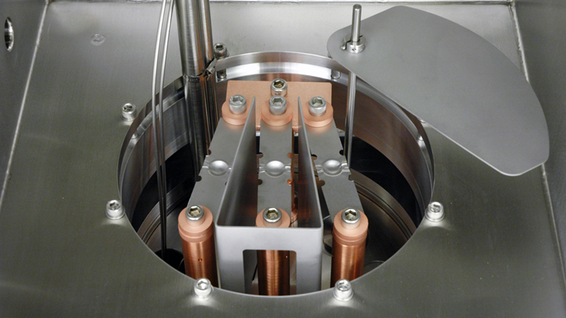
Precision thin-film deposition platforms engineered around the demands of today's most advanced applications. From quantum computing and superconducting devices to next-generation photovoltaics and 3D flip-chip interconnects.
Choose Your Application Series
Quanta Series
Superconducting & Quantum Computing Devices
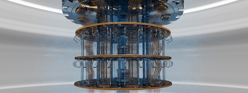
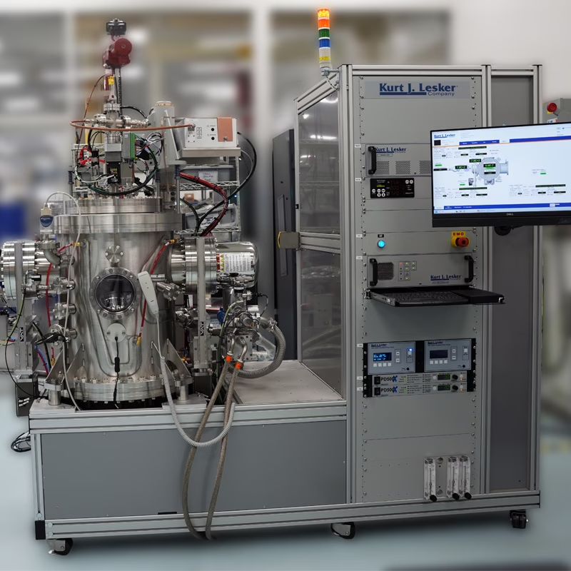
Ultra-high vacuum thin-film deposition platforms engineered for Josephson junctions, superconducting circuits, and low-loss interconnects. Covers e-beam evaporated aluminum JJs, UHV sputtering of superconducting metals and reactive compounds, and high-rate indium bump bonding for 3D integration. All systems are compatible with UHV transfer solutions for next-generation quantum device fabrication.
Perovskite Series
Solar Cells & Next-Gen Photovoltaics
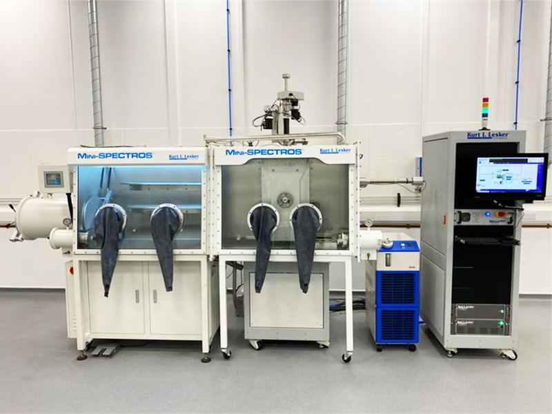
An advanced thin-film deposition platform engineered for substrates up to 210mm x 210mm, extending the SPECTROS architecture with a chamber optimized for vacuum-based perovskite deposition. Features enhanced pump protection, cooling shrouds, and up to 16 low-temperature evaporation sources (50–600°C) to handle volatile precursors. Supports glovebox integration, co-deposition, load lock, and ALD for barrier layers.
Indium Series
Flip-Chip Bump Bonding & 3D Integration
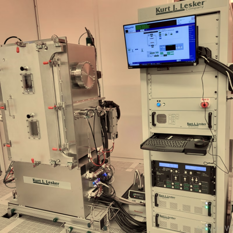
Purpose-built for indium bump bonding on wafers up to 200mm, delivering deposition rates exceeding 100 Å/sec with films up to 20 µm thick. LN2-cooled substrates promote high aspect-ratio out-of-plane growth essential for robust flip-chip interconnects in superconducting quantum circuits. Up to four high-capacity thermal sources, specialized shielding, and flux monitoring enable up to 10 wafers per pump cycle.
TSV/TGV Series
Through Silicon Via & Through Glass Via Metallization
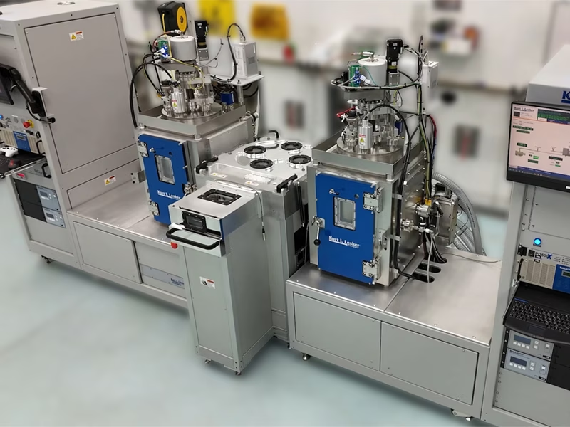
Purpose-built for depositing adhesion, barrier, and seed layers into high-aspect-ratio (up to 8:1) Through Silicon Vias and Through Glass Vias. A technically superior chamber design paired with KJLC's TORUS MagKeeper FFE sputter sources and HiPIMS ionization delivers excellent step coverage and uniformity deep inside complex via structures. The eKLipse™ software control system enables stable, high-rate deposition, allowing up to 10 wafers to be processed before breaking vacuum. Available as single-chamber systems or fully integrated cluster tools with robotic transfer, pre-clean, and dedicated barrier/seed modules.
Space Simulation Series
Thermal Vacuum Chambers for Aerospace Testing
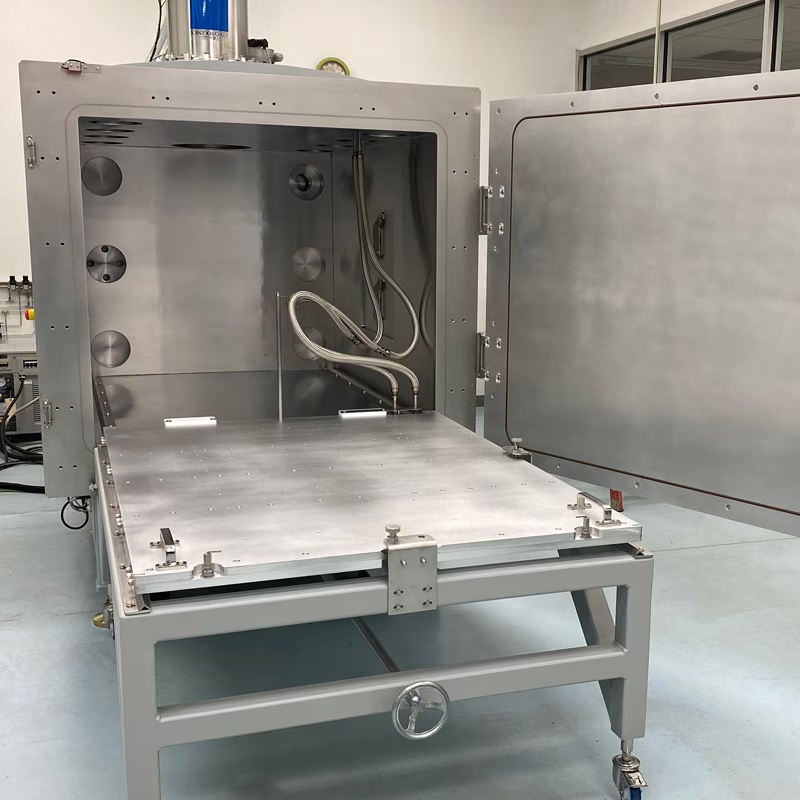
Scalable Thermal Vacuum Chamber (TVAC) platforms engineered to replicate the deep vacuum and extreme thermal conditions of outer space. Systems range from compact CubeSat-scale chambers to large cylindrical enclosures for full satellite assemblies, achieving pressures from 10-6 to 10-8 Torr. Programmable thermal cycling from -100°C (LN2) to +250°C, optional solar/radiation simulation, and full eKLipse-driven recipe automation support qualification, validation, and life-cycle testing of aerospace hardware.
Ready to Advance Your Research?
Do you have any questions? Click below to get in contact with one of our many experienced team members.