October 25, 2017 | By KJLC Innovate

In a July 2017 publication, Drs. André Anders and Yuchen Yang provide an enhanced description of the flows and energy of electrons at the face of a magnetron sputter cathode. By combining a unique imaging process and a linear cathode (target) the researchers were able to generate a series of time/space images which shows plasma instabilities driven by the motion of electrons, within the cathode's magnetic field. The images show the effects on plasma flow for both conventional DC magnetron sputtering (dcMS) and also high power impulse magnetron sputtering (HiPIMs). The full paper is available on line at http://aip.scitation.org/doi/10.1063/1.4994192.
Read More
Tags:
INNOVATE
Vacuum Science
Deposition Techniques
May 15, 2017 | By KJLC Blog

With the dramatic growth expected in many industries which require high temperature vacuum systems such as space simulation systems, 3D printing of metal components, the manufacture of single crystals for the LED and semiconductors and others, alternatives to traditional water cooling approaches may offer performance gains coupled with reduced costs. Temperature control for these applications can take several forms. In the case of space simulation, the vacuum system is designed to duplicate the temperature (and pressure) extremes that will be experienced by satellites in earth orbit, or beyond, which may require rapid cycling from -130°C to +130°C. For crystal growing, using methods such as the Kyropoulos process, where a crystal is 'pulled' from a melt of material, such as silicon, the internal temperature of a vacuum system may reach +1,450°C. In one case, the temperature control system for the vacuum chamber is designed to provide a user-specified profile of cold-to-hot and in another the system is required to safely mitigate and protect the system from the extreme temperature required to liquify silicon.
Read More
Tags:
Vacuum Science
February 20, 2017 | By KJLC Innovate
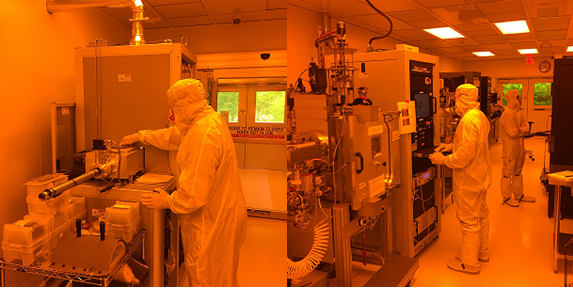
Next generation vacuum deposition systems must evolve in order to keep pace with the ongoing evolution of thin film materials and devices. Researchers seeking to pursue new areas, such as biomedical devices, 2D materials, specialized magnetics and oxide-based films need new tools to support their work. The frontiers of materials science, particularly at the intersection of biology and thin film deposition, have brought new materials into the vacuum space that were never intended to be there.
Read More
Tags:
INNOVATE
Systems
Vacuum Science
Deposition Techniques
December 30, 2016 | By KJLC Blog
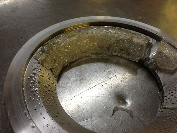
Users of diffusion pumps for harsh processes or in non-optimized vacuum systems may be seeing crystallization of solids in their pump fluid. This crystallization results from decomposition of fluids due to over exposure to oxygen at high temperatures. This break down alters the viscosity of the pump fluid and may also obstruct flow passages. Further, the build-up of solids and crystals on internal surfaces can lead to inefficient heat transfer which may make operation of the pump unstable.
Read More
Tags:
Vacuum Fluids & Greases
Vacuum Science
August 30, 2016 | By KJLC Innovate
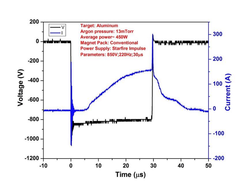
High Power Pulsed Magnetron Sputtering (HPPMS) or High Power Impulse Magnetron Sputtering (HIPIMS) is a type of magnetron sputtering technique where high power pulses of hundreds of microseconds are applied to the magnetron target at frequencies ranging from a few Hz to several kHz.
Read More
Tags:
INNOVATE
Systems
Vacuum Science
May 13, 2016 | By KJLC Innovate

Solar cells work by using materials that absorb photons from sunlight in a broad spectral range and in turn effectively convert this captured light into free charges that produce electricity. Modern solar cells are based on crystalline Silicon (c-Si) which is a cheap and abundant semiconductor, however the cost to produce electricity using them is relatively high as the efficiency rates of c-Si based cells are relatively low. As a result thin film solar cells have been developed to combat crystalline Silicon's inherent inefficiencies. Technologies such as CIGS, CdTE, amorphous Silicon and OPV have all strived to create solar cells that have high efficiencies coupled with good cell stability and low manufacturing costs.
Read More
Tags:
INNOVATE
Systems
Vacuum Science
May 09, 2016 | By KJLC Innovate

ALD has been described as a thin film deposition technology that can keep the semiconductor industry on track per Moore's law (or observation) [1] for a few more years. In its most ideal form, it is a process that enables monolayer, or sub-monolayer growth of certain materials through the sequential exposure of a functionalized substrate to a pair of precursor gases. If dosed correctly the gases attach at specific surface sites and react to create a near perfect film on the order of a few angstroms thick. Presently the U.S. Department of Defense anticipates that the last process node for semiconductor devices (the end of Moore's) is 7 nm and will be achieved by 2020 [2].
Read More
Tags:
INNOVATE
Systems
Vacuum Science
Deposition Techniques
January 19, 2016 | By KJLC Innovate
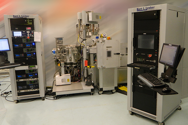
Combinatorial Magnetron Sputtering (CMS) has distinguished itself as a viable tool for the rapid development of vast libraries of complex materials. Researchers at the Joint Center for Artificial Photosynthesis, California Institute of Technology (Cal Tech) and the Kurt J. Lesker Company® (KJLC®) [1] have recently published work on Combinatorial Magnetron Sputtering (CMS) using a novel robotically controlled thin film deposition cathode tilt and substrate manipulation mechanism. Combinations of metal alloys, mixed metal oxides and nitrides have been demonstrated with the system as a basis for a predictive model developed by Cal Tech to streamline the design of new materials for certain critical applications.
Read More
Tags:
INNOVATE
Systems
Vacuum Science
Deposition Techniques
July 29, 2015 | By KJLC Innovate
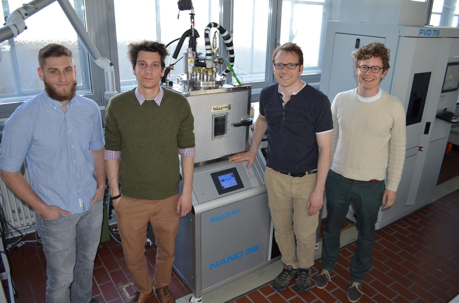
Plasmonics is an important field of research with applications in bio-sensing, photocatalysis, solar cells and high-speed computing, among others. The fundamental technologically enabling features of plasmonics are sub-wavelength confinement of electromagnetic fields and ultra-strong enhancement of those fields. Highly-reflective metals are the predominant material choice for plasmonic devices. More specifically, Gold and Silver have been the most studied materials to date. Aluminum and Copper are burgeoning plasmonic materials which offer CMOS compatibility and low cost. Furthermore, Aluminium opens up the possibility of ultraviolet plasmonic devices which have recently been shown to have applications in bio-sensing and colour filters.
Read More
Tags:
INNOVATE
Systems
Vacuum Science
March 30, 2015 | By KJLC Innovate
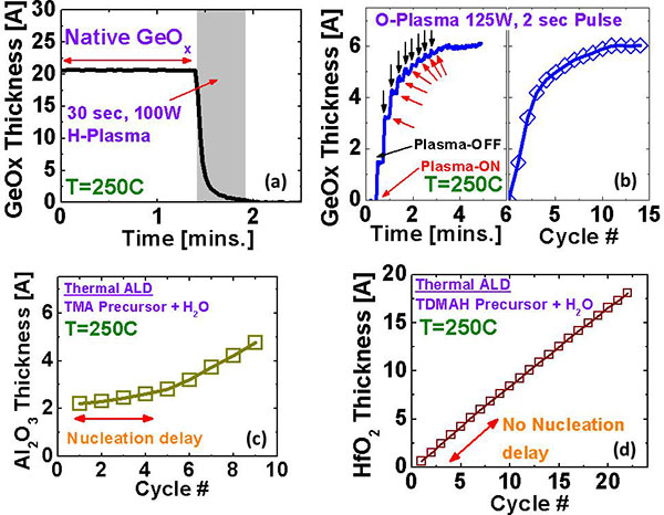
Germanium (Ge) is a promising candidate to enhance p-channel metal oxide silicon field transistor (MOSFET) device performance. The successful development of Ge-based field effect devices requires the integration of a high-quality dielectric with equivalent oxide thickness (EOT) less than 1 nanometer that forms an electrically well behaved semiconductor dielectric interface. Although GeOx/Ge has been found promising, the thermodynamic instability as well as the relatively low dielectric constant of GeOx requires an alternative approach. The utilization of an ultrathin Si layer, to modify the semiconductor-dielectric interface from Ge into Si, is a viable approach that has been successfully demonstrated; however, the introduction of a thin Si layer into the gate stack is incompatible with the 3D FinFET manufacturing process flow and also leads to increased EOT. It is, therefore, desirable to develop a multilayer gate-stack by atomic layer deposition (ALD), where an ultrathin GeOx layer can be thermodynamically stabilized and combined with a high-k dielectric film to meet the stringent requirement of low interface trap density and large capacitance density while maintaining a low gate leakage under the constraint of full compatibility with modern 3D FinFET geometries.
Read More
Tags:
INNOVATE
Systems
Vacuum Science
Previous Entries
Next Entries